Punjab State Board PSEB 12th Class Physics Book Solutions Chapter 14 Semiconductor Electronics: Materials, Devices, and Simple Circuits Textbook Exercise Questions and Answers.
PSEB Solutions for Class 12 Physics Chapter 14 Semiconductor Electronics: Materials, Devices, and Simple Circuits
PSEB 12th Class Physics Guide Semiconductor Electronics: Materials, Devices, and Simple Circuits Textbook Questions and Answers
Question 1.
In an n-type silicon, which of the following statement is true:
(a) Electrons are majority carriers and trivalent atoms are the dopants.
(b) Electrons are minority carriers and pentavalent atoms are the dopants.
(c) Holes are minority carriers and pentavalent atoms are the dopants.
(d) Holes are majority carriers and trivalent atoms are the dopants.
Answer:
The correct statement is (c).
In an n-type silicon, the electrons are the majority carriers, while the holes are the minority carriers.
An n-type semiconductor is obtained when pentavalent atoms, such as phosphorus, are doped in silicon atoms.
Question 2.
Which of the statements given in Exercise 14.1 is true for p-type semiconductors.
Answer:
The correct statement is (d).
In a p-type semiconductor, the holes are majority carriers, while the electrons are the minority carriers.
A p-type semiconductor is obtained when trivalent atoms, such as aluminum, are doped in silicon atoms.
Question 3.
Carbon, silicon, and germanium have four valence electrons each.
These are characterized by valence and conduction bands separated by energy bandgap respectively equal to (Eg)C, (Eg) si, and (Eg)Ge Which of the following statements is true?
(a) (Eg)si<(Eg)Ge<(Eg)C
(b) (Eg)C<(Eg)Ge>(Eg)Si
(c) (Eg)C > (Eg)Si > (Eg)Ge
(d) (Eg)C =(Eg)Si = (Eg)Ge
Answer:
The correct statement is (c).
Out of the three given elements, the energy band gap of carbon is the maximum and that of germanium is the least.
The energy band gap of these elements are related as (Eg)C > (Eg)Si > (Eg)Ge.
![]()
Question 4.
In an unbiased p-n junction, holes diffuse from the p-region to n-region because
(a) free electrons in the n-region attract them.
(b) they move across the junction by the potential difference.
(c) hole concentration in p-region is more as compared to n-region.
(d) All of the above.
Answer:
The correct statement is (c).
The diffusion of charge carriers across a junction takes place from the region of higher concentration to the region of lower concentration. In this case, the p-region has greater concentration of holes than the n-region. Hence, in an unbiased p-n junction, holes diffuse from the p-region to the n-region.
Question 5.
When a forward bias is applied to a p-n junction, it
(a) raises the potential barrier,
(b) reduces the majority carrier current to zero,
(c) lowers the potential barrier.
(d) None of the above.
Answer:
The correct statement is (c).
When a forward bias is applied to a p-n junction, it lowers the value of potential barrier.
In the case of a forward bias, the potential barrier opposes the applied voltage.
Hence, the potential barrier across the junction gets reduced.
Question 6.
For transistor action which of the following statements are correct:
(a) Base, emitter and collector regions should have similar size and doping concentrations.
(b) The base region must be very thin and lightly doped.
(c) The emitter junction is forward biased and collector junction is reverse biased.
(d) Both the emitter junction as well as the collector junction are forward biased.
Answer:
The correct statements are (b) and (c).
For a transistor action, the junction must be lightly doped so that the base region is very thin.
Also, both the emitter junction must be forward-biased and collector junction should be reverse-biased.
Question 7.
For a transistor amplifier, the voltage gain
(a) remains constant for all frequencies.
(b) is high at high and low frequencies and constant in the middle-frequency range.
(c) is low at high and low frequencies and constant at mid frequencies.
(d) None of the above.
Answer:
The correct statement is (c).
The voltage gain of a transistor amplifier is constant at mid-frequency range only. It is low at high and low frequencies.
![]()
Question 8.
In half-wave rectification, what is the output frequency if the input frequency is 50 Hz.
What is the output frequency of a full-wave rectifier for the same input frequency.
Answer:
Input frequency = 50 Hz
For a half-wave rectifier, the output frequency is equal to the input frequency.
∴ Output frequency = 50 Hz
For a full-wave rectifier, the output frequency is twice the input frequency
∴ Output frequency = 2 x 50 = 100 Hz
Question 9.
For a CE-transistor amplifier, the audio signal voltage across the collected resistance of 2 kΩ is 2V.
Suppose the current amplification factor of the transistor is 100, find the input signal voltage and base current, if the base resistance is 1 kΩ.
Answer:
Given, Rc = 2 kΩ, RB = 1 kΩ,
V0 = 2V, input voltage Vi = ?
β = \(\frac{I_{C}}{I_{B}}\) = 100
V0=ICRC= 2V
ic = \(\frac{2 V}{R_{C}}=\frac{2 \mathrm{~V}}{2 \times 10^{3} \Omega}\) = 1.0-3 A.
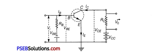
Base current,
IB = \(\frac{I_{C}}{\beta}=\frac{10^{-3}}{100}\) = 10 x 10-6 A = 10 μA
Base current, RB = \(\frac{V_{B B}}{I_{B}}\)
Input Voltage, Vi = RB x IB
= 1 x 103 x 10 x 10-6
= 0.01 V
Question 10.
Two amplifiers are connected one after the other in series (cascaded). The first amplifier has a voltage gain of 10 and the second has a voltage gain of 20. If the input signal is 0.01 volt, calculate the output ac signal.
Answer:
Voltage gain of the first amplifier, V1 = 10
Voltage gain of the second amplifier; V2 = 20
Input signal voltage, Vi = 0.01V
Output AC signal voltage = V0
The total voltage gain of a two-stage cascaded amplifier is given by the product of voltage gains of both the stages, Le.,
V = V1 x V2=10 x 20 =200
We have the relation
V0 =V x Vi= 200 x 0.01 = 2 V
Therefore, the output AC signal of the given amplifier is 2 V.
Question 11.
A p-n photodiode is fabricated from a semiconductor with bandgap of 2.8 eV. Can it detect a wavelength of 6000 nm?
Answer:
Energy band gap of the given photodiode, Eg = 2.8 eV
Wavelength, λ = 6000 nm= 6000 x 10-9m
The energy of a signal is given by the relation
E = \(\frac{h c}{\lambda}\)
where, h = Planck’s constant = 6.63 x 10⁻³⁴ Js
c = Speed of light = 3 x 10⁸ m/s
E = \(\frac{6.63 \times 10^{-34} \times 3 \times 10^{8}}{6000 \times 10^{-9}}\) = 3.313 x 10⁻²⁰ J
But 1.6 x 10⁻¹⁹ J = 1 eV
E = \(\frac{3.313 \times 10^{-20}}{1.6 \times 10^{-19}}\) = 0.207 eV
Additional Exercises
Question 12.
The number of silicon atoms per m3 is 5 x 1028.
This is doped simultaneously with 5 x 10²² atoms per m3 of Arsenic and 5 x 10²⁰ per m3 atoms of Indium.
Calculate the number of electrons and holes. Given that ni= 1.5 x 10¹⁶m-3. Is the material n-type or p-type?
Answer:
Arsenic is n-type impurity and indium is p-type impurity.
Number of electrons, ne = nD – nA
= 5 x 10²² – 5 x 1020 = 4.95 x10²² m-3
Also, ni = nenh
Given, ni =1.5 x 10¹⁶ m-3
Number of holes, nh=\(\frac{n_{i}^{2}}{n_{e}}\) = \(\frac{\left(1.5 \times 10^{16}\right)^{2}}{4.95 \times 10^{22}} \)
⇒ nh =4.54 x 10⁹ m-3
As ne > nh. so the material is an n-type semiconductor.
![]()
Question 13.
In an intrinsic semiconductor, the energy gap Eg is 1.2 eV. Its hole mobility is much smaller than electron mobility and independent of temperature. What is the ratio between conductivity at 600K and that at 300K? Assume that the temperature dependence of intrinsic carrier concentration ni is given by ni = n0 exp\(\left[-\frac{E_{g}}{2 k_{B} T}\right]\) where n0 is a constant.
Answer:
Energy gap of the given intrinsic semiconductor, E = 1.2 eV
The temperature dependence of the intrinsic carrier-concentration is written as
ni = n0 exp\(\left[-\frac{E_{g}}{2 k_{B} T}\right]\)
where, kB = Boltzmann constant = 8.62 x 10⁻⁵eV/K
T = Temperature, n0 = Constant
Initial temperature, T1 = 300 K
The intrinsic carrier-concentration at this temperature can be written as
ni1 =n0exp \(\left[-\frac{E_{g}}{2 k_{B} \times 300}\right]\)
………………………….. (1)
Final temperature, T2 = 600 K
The intrinsic carrier-concentration at this temperature can be written as
ni1 = n0exp \(\left[-\frac{E_{g}}{2 k_{B} \times 600}\right]\)
………………………………… (2)
The ratio between the conductivities at 600 K and at 300 K is equal to the ratio between the respective intrinsic carrier- concentrations at these temperatures.
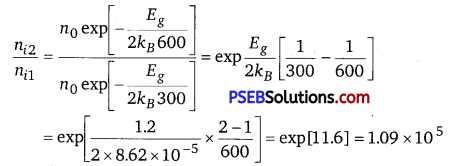
Therefore, the ratio between the conductivities is 1.09 x 10⁵.
Question 14.
In a p.n junction diode, the current I can be expressed as
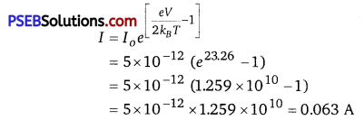
I = I0exp\(\left(\frac{\mathrm{eV}}{2 k_{B} T}-1\right)\) where I0 is called the reverse saturation current, V is the voltage across the diode and is positive for forward bias and negative for reverse bias, and I is the current through the diode, kB is the Boltzmann constant (8.6 x 10⁻⁵ eV/K) and T is the absolute temperature. if for a given diode I0 = 5 x 10-12 A and T = 300K, then
(a) What will be the forward current at a forward voltage of 0.6V?
(b) What will be the increase in the current if the voltage across the diode is increased to 0.7 V?
(c) What is the dynamic resistance?
(d) What will be the current if reverse bias voltage changes from 1V to 2 V?
Answer:
Given, I0 = 5 x 10-12 A, T = 300 K
kB =8.6 x 10⁻⁵ eV/K
= 8.6 x 10-5 x 1.6 x 10-19J/K
(a) Given, voltage V = 0.6 V
∴ \(\frac{e V}{k_{B} T}=\frac{1.6 \times 10^{-19} \times 0.6}{8.6 \times 10^{-5} \times 1.6 \times 10^{-19} \times 300}\) = 23.26
The current I through a junction diode is given by
(b) Given, voltage V = 0.7 V
∴ \( \frac{e V}{k_{B} T}=\frac{1.6 \times 10^{-19} \times 0.7}{8.6 \times 10^{-5} \times 1.6 \times 10^{-19} \times 300}\) = 27.14
Now,
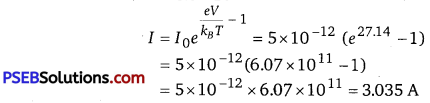
Change in current ΔI = 3.035 — 0.063 = 2.9 A
(c) ΔI =2.9 A, voltage ΔV=0.7—0.6=0.1 V
Dynamic resistance Rd =\(\frac{\Delta V}{\Delta I}=\frac{0.1}{2.9}\) = 0.0336 Ω
(d) As the voltage changes from 1 V to 2 V, the current I will be almost
equal to I0 = 5 x 10-12 A.
It is due to that the diode possesses practically infinite resistance in the reverse bias.
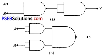
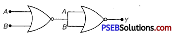
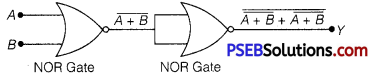
Question 15.
You are given the two circuits as shown in Fig. 14.44. Show that
circuit (a) acts as OR gate while the circuit (b) acts as AND gate.
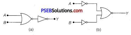
Answer:
(a) A and B are the inputs and Y is the output of the given circuit. The left half of the given figure acts as the NOR Gate, while the right half acts as the NOT Gate. This is shown in the following figure
Hence, the output of the NOR Gate = \(\overline{A+B}\)
This will be the input for the NOT Gate. Its output will be \(\overline{\overline{A+B}}\) = A+B
∴ Y = A + B
Hence, this circuit functions as an OR Gate.
(b) A and B are the inputs and Y is the output of the given circuit. It can be observed from the following figure that the inputs of the right half NOR Gate are the outputs of the two NOT Gates.
Hence, the output of the given circuit can be written as
Y = \(\overline{\bar{A}+\bar{B}}=\overline{\bar{A}} \cdot \overline{\bar{B}}= \) = A.B
Hence, the circuit functions as an AND Gate.
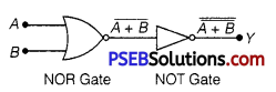
Question 16.
Write the truth table for a NAND gate connected as given in Fig. 14.45. Hence identify the exact logic operation carried out by this circuit.
Answer:
A acts as the two inputs of the NAND gate and Y is the output, as shown in the following figure
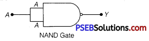
Hence, the output can be written as
Y =\(\overline{A \cdot A}=\bar{A}+\bar{A}=\bar{A}\) ……………………… (1)
The truth table for equation (1) can be drawn as
| A | Y = \(\bar{A}\) |
| 0 | 1 |
| 1 | 0 |
This circuit functions as a NOT gate. The symbol for this logic circuit is shown as

![]()
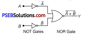
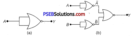
Question 17.
You are given two circuits as shown in Fig. 14.46, which consist of NAND gates. Identify the logic operation carried out by the two circuits.
Answer:
In both the given circuits, A and B are the inputs and Y is the output
(a) The output of the left NAND gate will be A. B, as shown in the following figure
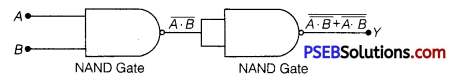
Hence, the output of the combination of the two NAND gates is given as
Y= \(\overline{(\overline{A \cdot B}) \cdot(\overline{A \cdot B})}=\overline{\overline{A B}}+\overline{\overline{A B}}\) =AB
Hence, this circuit functions as an AND gate.
(b) \(\bar{A}\) is the output of the upper half of the NAND gate and B is the output of the lower half of the NAND gate, as shown in the following figure
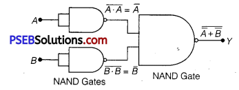
Hence, the output of the combination of theNAND gates will be given as
Y = \(\bar{A} \cdot \bar{B}=\overline{\bar{A}}+\overline{\bar{B}}\) =A + B
Hence, this circuit functions as an OR gate.
Question 18.
Write the truth table for circuit given in Fig 14.47 below consisting of NOR gates and identify the logic operation (OR, AND, NOT) which this circuit is performing.
(Hint: A = 0, B = 1 then A and B inputs of second NOR gate will be 0 and hence Y = 1. Similarly, work out the values of Y for other combinations of A and B. Compare with the truth table of OR, AND, NOT gates and find the correct one.)
Answer:
A and B are the mputs of the given circuit The output of the first NOR gate ’ is \(\overline{A+B}\) .
It can be observed from the following figure that the inputs of the second NOR gate become the out put of the first one
Hence, the output of the combination is given as
Y= \(\overline{\overline{A+B}+\overline{A+B}}\)
= \(\overline{\bar{A}+\bar{B}}+\overline{\bar{A} \cdot \bar{B}}\)
= \(\overline{\bar{A} \cdot \bar{B}}=\overline{\bar{A}}+\overline{\bar{B}}\) = A+B
The truth table for this operation is given as
| A | B | Y(= A+B) |
| 0 | 0 | 0 |
| 0 | 1 | 1 |
| 1 | 0 | 1 |
| 1 | 1 | 1 |
This is the truth table of an OR gate. Hence, this circuit functions as an OR gate.
Question 19.
Write the truth table for the circuits given in Fig.14.48 consisting of NOR gates only. Identify the logic operations (OR, AND, NOT) performed by the two circuits.
Answer:
(a) A acts as the two inputs of the NOR gate and Y is the output, as shown in the following figure.
Hence, the output of the circuit is \(\overline{A+A}\)
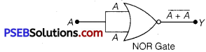
The truth table for the same is given as
| A | Y = \(\bar{A}\) |
| 0 | 1 |
| 1 | 0 |
This is the truth table of a NOT gate. Hence, this circuit functions as a NOT gate.
(b) A and B are the inputs and Y is the output of the given circuit. By using the result obtained in solution
(a), we can infer that the outputs of the
first two NOR gates are \(\bar{A}\) and \(\bar{B}\), as shown in the following figure
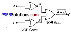
\(\bar{A}\) and \(\bar{B}\) are the inputs for the last NOR gate.
Hence, the output for the circuit can be written as
Y = \(\overline{\bar{A}+\bar{B}}=\overline{\bar{A}} \cdot \overline{\bar{B}}\) = A.B
The truth table for the same can be written as
| A | B | Y(=A.B) |
| o | o | o |
| o | 1 | o |
| 1 | 0 | 0 |
| 1 | 1 | 1 |
This is the truth table of an ANL) gate. Hence, this circuit functions as an AND gate.